In this post, I’m going to give you an overview of the Epiphany co-processor architecture, including the motivations for a co-processors and hardware accelerators, what sets co-processors apart, and then the details of the Epiphany co-processor.
While you may think that this post is not as important as the future posts that will walk you through how to run programs on the Epiphany chip, I urge you not to skip it. Understanding the architecture of any machine is crucial for properly programming it. Skip this post at your own risk. This post was adapted from my slides and lecture notes that I used to teach my students during the Epiphany unit we had this past semester.
Why co-processors?
Let’s start our discussion with chip design, which drives much of the hardware arhchitecture we have available to us. Driven by Moore’s law, chip manufacturers work laboriously to create smaller and smaller cores. The CPUs and the cores we are familiar with are heavy-duty, multi-purpose CPU cores, that support a wide range of tasks. To support such a wide range of operations, a lot of complexity goes into CPU design. With transistor technology stalling, computer and material engineers struggled to create smaller and smaller devices. Making such complex cores smaller is extremely hard, especially as power becomes the dominating limiting factor.
The answer that chip designers arrived at was to create “simplified” processors that are designed to perform very specialized tasks. Unlike general-purpose computing cores such as CPUs, simplified processing cores such as GPUs and Co-Processors cannot do all the things that regular CPUs can. Instead, they depend on a CPU (referred to as the host) to act in a supervisory role to the simplified processor (referred to as the device). They are connected to each other via communication channels such as DMA (direct memory access) and control in order to enable instructions and memory to flow between the device and the host. This workflow is the same regardless of whether or not you are dealing with a co-processor or a GPU. While these simplified processors cannot do the same range of tasks that CPUs can, they are excellent at many, and are much more energy efficient than a standard CPU.
What makes a co-processor different from a GPU?
Like the GPU, the Co-Processor is a simplified processor. Most importantly, it cannot independently fetch memory or do I/O operations. It depends on a closely supervising host CPU to do these tasks. However, co-processors are advertised as being a “simpler” CPU, with an architecture that is more similar to the CPU than the GPU is.
This is one of the main sellings points of the Intel Xeon Phi chip that was released in 2012. Cores are networked together on the chip, allowing for arguably a greater range of operations than the SIMD GPUs. Co-processors typically follow the MIMD architecture. The Intel Xeon Phi chip made headlines when it was incorporated into the world’s fastest supercomputer, the Tianhe 2. The Tianhe 2 supercomputer has been at the top of the Supercomputing Top500 list for two years in a row, an unheard of achievement.
One of the consequences of having a similar architecture to the x86 architecture, is that the Intel Xeo Phi chips should be easier to program, as languages and libraries used on CPUs (C/Fortran, Pthreads, OpenMP, MPI) can also used to program the Phi chips. As such, the chip is being advertised as being potentially easier to program than GPUs.
Nvidia for its part has been wholly unimpressed. Recent bencmarks suggest that some of NVidia’s GPUs outstrip the Xeon Phi in performance. NVidia also contends that in order to get any “real” performance out of the Phi, you will need use low-level primatives similar to what you use in CUDA. In other words, there is no free lunch. As GPGPUs continue to increase in sophistication, GPUs become less SIMD like and more MIMD like.
However, the Phi co-processor technology is fairly new, and the argument can be made that the “ease” of programming the chip is a worthwhile tradeoff for increased performance in many cases. This brings us to the Epiphany chip, a novel co-processor that is developed by Adapteva and is included on every Parallella board.
The Epiphany Architecture
Let’s take a closer look at the Epiphany architecture. To fully understand what is going on here, we will need to take a look at two things: the chip’s internal layout/communication model, and memory organization
Chip layout
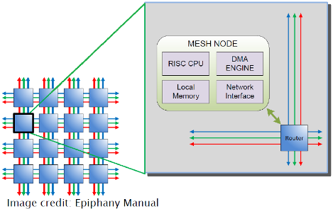
The figure below gives an overview of the layout and communication model of the Epiphany chip.
The chip is composed of sixteen “nodes” arranged in a 4 × 4 mesh, where each node in the mesh contains a epiphany core, DMA engine, 32KB of local memory, and network interface. The mesh allows the nodes to communicate very quickly with each other.
Each node also has an id, which is determined by its (row,col) index in the
mesh. Each core can access any other core by using this coordinate system.
Another consequence of this organization is that each core could be
theoretically programmed to run different tasks. This is one of the reasons
why the Epiphany architecture is a MIMD architecture, unlike the SIMD
architecture found in the GPUs.
Memory structure
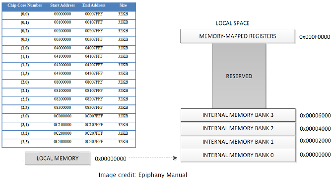
The figure below gives an overview of of the memory layout of each memory bank on the Epiphany chip.
The memory is a single flat, little-endian address space which is organized to reflect the mesh layout of the ephiphany cores. Each node has an individual bank of memory of 32KB. On each node, local memory is organized into 4 8KB banks. For optimal performance it is suggested that data be placed into separate banks. Please note that these banks of local memory are NOT caches, as there is no established coherence policy between them. There is additional space reserved for expansion, but is not currently addressed. There is also some additional space reserved for the 64 local registers. 8-bit, 16-bit, 32-bit and 64-bit integer (int and char) data types are supported, along with 32-bit floating point numbers (float). Doubles are NOT supported and should be avoided.

